

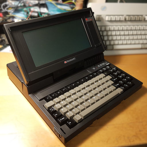
Something that always stuck out to me with my Bondwell B310 laptop was the claim of "1MB of memory (expandable to 2MB)" in the sale literature for it. My model, like every other one I've seen or heard about online is the 1MB base model. I would speculate that close to 100% of them left the factory like that as very few DOS users would have been able to take advantage of more than 640kB anyways. Especially on a 286 where accessing XMS was a little more difficult for applications, compared with the 386 and later. However, some things did make use of that, such as Windows, OS/2, and some UNIX OS's — as well some applications will make use of it, such as 4DOS, and EMS emulators such as EMS286 can make this memory available to applications that can use EMS.
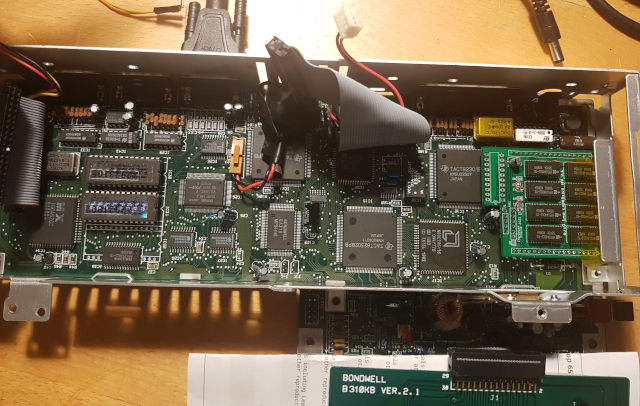
Having previously opened this laptop up a few times, originally for curiousity, then later to fully recap the machine as failing capacitors in the PSU section were causing screen contrast issues that were rendering it unusable, I knew that there indeed was a header for ram expansion right on top of the onboard memory chips. However, the problem was that it was a proprietary expansion and not just empty ram sockets, or a SIMM or SIPP module. Two 18-pin headers were placed, one on either side of the 8—256k by 4-bit dram modules that made up the base 1MB of RAM. With no photographic reference or service manual or schematics for the Bondwell B310 to be found it was up to me to reverse engineer this.
As a first check I had gone searching for any mention of this board on the internet, but all I was able to find were sales broshures and magazine advertisements that mentioned the possibility of 2MB of ram, but never even a picture of one. With my experiance in creating and installing such an expansion, I believe this could only have been a factory option, or if it was available as a later upgrade it would have to have required sending the machine back to the factory. This is due to installing the board requiring a complete disassembly of the machine down to the bare boards, removing all the internal frame, drives, and heatsink mount to get to the socket enough to install a board into it.
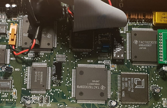
So without an original to go off of, reverse engineering was the approach I had to take. Another difficulty here being the lack of service manuals, schematics, or even a user manual for the laptop available or online. Taking the laptop apart I was able to start looking around for other clues. The chipset of the laptop is a Ti TACT82301BPB / TACT82302BPB / TACT82303BPB, 3-chip AT chipset. Unfortunatly after digging into this I was unable to find the datasheet for this chipset, only a later TACT83000 "Tiger" chipset for a 386SX system, which was not particularilly helpful. According to dosdays.co.uk the 82301 is the system unit, the 82302 is the memory control unit, and 82303 is the peripheral control unit—as well the page also provides a quote from an Computer Business Review article, and mention that the chipset was also used in the Olivetti PCS 286. Looking for schematics or a service manual for that computer also proved fruitless. So it seemed that the chipset itself was a bust and I'd have to work around it. If anyone reading this does come across a datasheet for this chipset I'd still love to get it in the hopes of possibly increasing the RAM beyond 2MB or perhaps even hacking other things into this laptop.
|
Okay so no schematics, no pictures, and as well one more wrench thrown in the mix. Besides off the shelf chips and chipsets the laptop also contains a chip labelled "BONDWELL GA310 MP04446" which appears to be a gate array or CPLD of some kind (Possibly the GA in the markings), and is custom to this laptop. So the exact operations of this chip are and will always be unknown without some extreme effort—a black box.
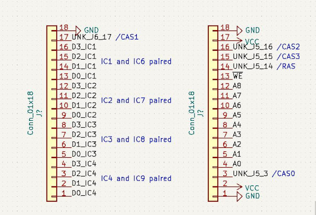
My course now was to pinout the connector to the best of my abilities. A VCF Forum post from 2016 references another user having at least some success in partly pinning out the ram connectors. Svenska was able to trace out 16 data lines, 9 address lines, /WE, three ground and 2 VCC pins. Leaving 5 pins unknown. This gave me hope that the matter wouldn't be too difficult and perhaps I could learn those missing pins. So I then set to work myself in tracing out these connectors.
Tracing out went relatively straight forward, I had pulled up a datasheet for the LH604256K DRAMs used on the mainboard, and started by pinning out the connector by searching for continuity from the pins to those DRAM ICs, figuring that the data bus, and address lines would be commoned with those. This hunch turned out to be correct and I was able to track down the same data that Svenska had mentioned in their post; 16 data lines (the 286 is a 16-bit system after all), 9 address lines (A0-A8, DRAM addresses are multiplexed and 18 address lines gives 256k addresses, combined with /RAS and /CAS lines providing chip selection), a /WE signal, three ground, and 2 VCC pins. Now I had to solve the unknowns.
I knew there had to be /RAS and /CAS lines for the DRAM chips. By looking at the chips on the mainboard I found they were grouped into 4 chips to a single /RAS line, for 2 /RAS, and then each pair of chips that make a byte were controlled by a /CAS line for 4 /CAS lines. This confused me as the decoding was overkill, either 1 /RAS and 4 /CAS, or 2 /RAS and 2 /CAS would be sufficient for the onboard chips. As well there were not 6 remaining pins on the expansion header to match this configuration, and none of these had continuity. Something was up.
I'd traced 4 of the 5 unknown pins from the expansion header over to the BONDWELL gate array chip, a dead end. However one pin was stubborn. with some more probing I found it's destination, one of the pins on the nearby 2-position resistor block socket was connected to it. Moving that resistor block over to the other position showed it now having a 150 ohm path to the /RAS1 line board of the main ram (/RAS1 being the name I gave to /RAS line on the second bank of RAM chips on the right edge of the board). Interestingly enough when experimenting before with the laptop I'd found that moving that jumper block to the other position resulted in the laptop only showing up with 512kB of RAM and I had assumed that perhaps it was there for machines shipped with only that much RAM? Either way with this discovery I was quite confident that the pin I found must be the /RAS line, and that the other 4 must be the /CAS lines in some way.
|
However, my confidence of the ordering of the /CAS lines, or if there was some extra decoding at play to get back a second (unneeded) /RAS line led me to not have 100% confidence in them. While those 5 lines are enough for the DRAM chips it didn't quite match what was on the mainboard. None the less I started making up a schematic based on what I had found. For DRAM chips I designed the circuit to use the same style of 20/26 pin SOJ DRAM chips as were used on the original motherboard, I didn't have many of these to hand but I did have the 1MBx4 replacements to these on a number of 4MB 72pin SIMM modules in the same SOJ form factor. These chips act completely the same as the original 256kx4 modules but add an extra A9 address line to a NC pin on the original. So with that pin held in a constant state these chips would behave identically to 256kx4 modules and either could be populated to my board.
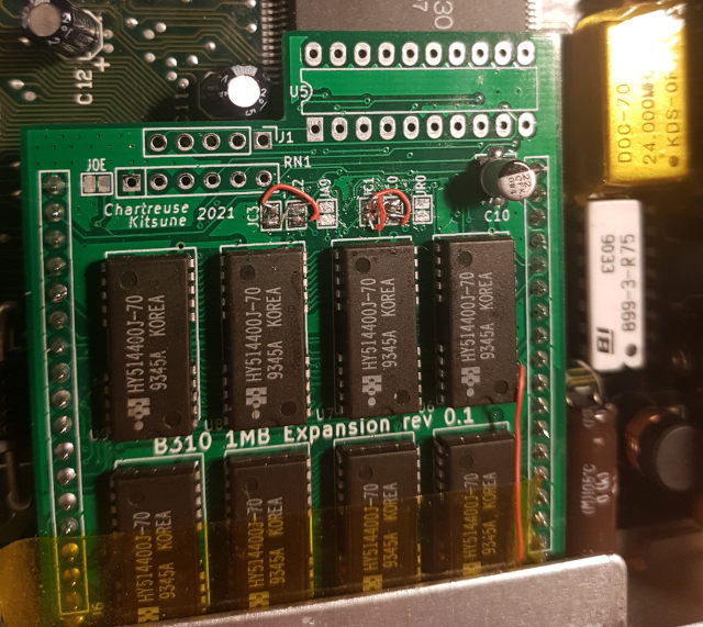
Due to my hesitancy with the 5 unknown pins I decided to play it safe on this PCB. I added the footprint for a 16V8 GAL programmable logic chip, a header for running wires down for any future need, as well as connecting the unknown pins and a few signals with cuttable jumper links on the PCB if I needed to reroute them. For the default state I went with my best guess. I'd connected the /RAS line I found to all 8 chips (with a cuttable jumper on the board in case I needed to split them). The 4 remaining unknowns I'd randomly assigned to /CAS pairs of chips. And the data pins were routed to the same chip placements as the mainboard used.
|
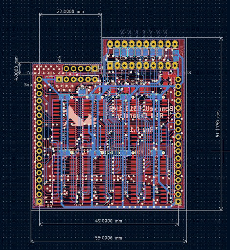
Now my experiance with designing PCBs has been rather minimal, only really making my 20x30 computer prototyping board earlier (as used on my 68010 homebrew that'll be posted shortly), and a couple small breakout boards that didn't even need schematics. For this project I was going to design a proper board in Kicad, based off a schematic and using surface mount parts (aside from the 16V8 GAL). I first started by getting the dimensions for the connectors correct, measuring the spacing using calipers. Surprisingly they weren't spaced on a nice multiple of 0.1". I then made the outline of the PCB to fit these connectors, and added a notched area to clear a tall capacitor on the board to fit the GAL. I then had to create footprints for the 20/26 pin SOJ RAM ICs and used KiCAD's built in footprint generator for this. While it worked out in the end the pads it generated were a little on the small side, and would not have worked if I were to have tried to solder the RAM chips using a standard soldering iron—f you were to make this yourself I would adjust the pads it generates to include an extra 2-3mm on the outside edges of the pads.
The next step was placing all the components on the board. I started by laying out the ram chips much the same way they were placed on the main board, and put them evenly spaced between the pin headers close to the bottom of the board. I allowed some room between them with the idea that I was going to hand solder the parts to the board, so they were placed as far apart as the board layout would allow. I then put the through hole 16V8 GAL footprint up by the notch and placed my cuttable jumpers just above the ram chips in a convinient location, as well placed the cut jumpers on the bottom side right below the GAL chip should I need to connect the lines to it. Just the extra header and a pull-up resistor pack for it remained, along with the 0.1uF bypass capacitors for each IC, and a 22uF bulk bypass cap for the whole board. Routing traces wasn't too bad for this 2 layer board. I chose to make the top layer mostly horizontal traces (for going between the RAM chips), and the bottom layer vertical traces, including power. The first thing I routed was the power lines to the RAM chips, knowing that they can be a real pain. I used plenty oversized 25 thou traces for the power lines and routed them in a two column setup down the middle of the ram chips, with ground coming from the bottom edge and VCC from the top. Then was a matter of connecting all the ram chips together which was a brease. As well as connecting the RAM chips to the edge connectors was quite smooth as well. Some of the difficulty came in linking the traces up to the cuttable jumpers, and the routing near the GAL became quite tight. It had gotten so bad at one point I scrapped all the routing in that area and redid it sticking to horizontal for the top and vertical for the bottom better in an attempt to make snaking traces with vias around much cleaner. Once everything was routed the final stage was to add in a copper fill for ground, and use more vias to stitch that together. To get that to my liking I did have to manually route in some extra ground traces and vias to get the plane over to some pockets. In the end I was quite happy with my PCB, and sent it of to be made by JLCPCB.
The PCB was made without issue in just a couple days, but ended up taking about 3 week to get here with the shipping. The boards looked great and I was quite hopeful to getting them to work, but put it off for a later date as I had some other, easier boards, made by someone else to assemble first. The other reason for the delay was that I had to use my hot air gun to desolder the RAM chips from the 72-pin SIMM and I wasn't super confident with it yet.
|
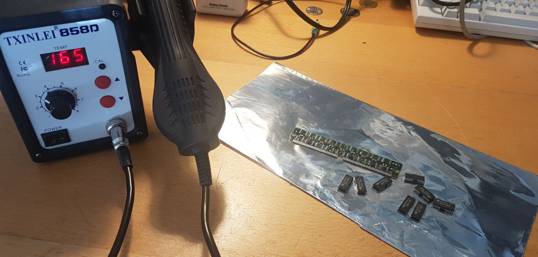
Fast forward to a few days ago, about a week after first recieving the boards I was ready to tackle them. I set up my workbench, using some aluminum foil to partly protect the wooden surface (I still need to get a silicone mat for doing this). Digging through my box of 72 pin SIMMs I found a number of candidates for 4MB donor modules (4MB modules use 8 1MBx4 DRAM chips, 1MB chips with 256kx4 chips are much less common, and I only had a pair of 256k 30 pin SIMMs). I selected the one with the least desirable characterestics for other systems; non-gold plated edge connectors, and 70ns DRAMs vs 60ns. Loading up the chips with good tack flux, and setting the hotair station to 380C (700F) which I'd had success with in my previous brief tests, and which is the same temp I tend to use on my iron for most soldering, I set to work. After slowly warming the whole board up by using the tool from a distance and circling the entire area, I moved in to start going after each chip. After chocking myself with the complete cloud of flux that formed—when doing hot air soldering all the flux kind of vaporizes at once compared with doing it with an iron where only a small amout is used—I decided to stop for a second and setup my fume extractor and open the window with a fan on low in it. Fair warning to those who've never done hot air work before, use good ventilation, it's much worse that normal single pin soldering. Resuming work on the board, after longer than I though moving the iron from side to side on the first chip I finally noticed the solder liquifying after getting the handle closer to the board, using some tweezers I was able to lift the first chip cleanly off the board. From there progress was quick in removing the subsequent 8 chips with ease.
It was at this point that I noticed my mistake in making the pads quite narrow on the board, and that I wouldn't be able to use an iron to solder the SOJ packages. With no real other option I decided it would be easiest to just solder them with hot air again. I didn't have solder paste which would be the normal method of doing this so what I did was to lightly (and importantly EVENLY!) tin each pad on the board, then generously apply flux to the board. This would allow the hot air to reflow the solder on each pad to adhere to the ram chips. Going big I decided to do all 8 chips at once, figuring it'd be less stress on the board and should be easy enough. Took a while to get the chips all nicely aligned with the pads. I did much the same as before while desoldering, slowly heating the board and all the chips before tackling them one by one. Overall went quite smoothly with an even bigger cloud of flux while working on it. Jumping ahead in the story and some debugging effort only one chip (the first one I started one) wasn't soldered quite right and a couple pins were floating ever so slightly above the board, more solder, reflowing and nudging it with tweezers was all it took to get it seated again. The rest of the components were done with a traditional iron.
![Board with all components soldered]](solderedchips_full.jpg)
|
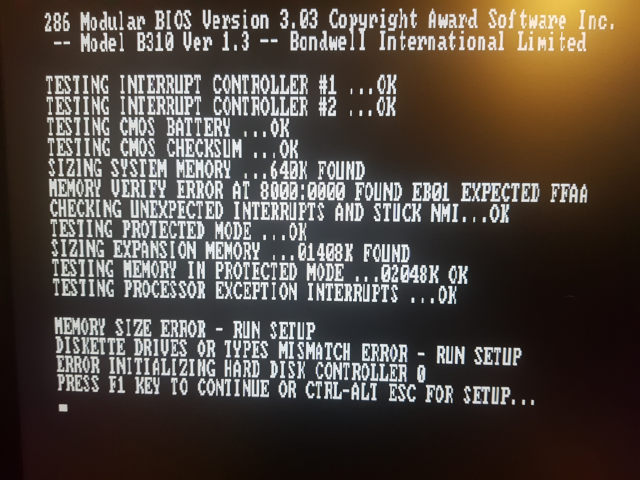
On to testing the board. After disassembling the computer and installing the RAM expansion it was on to testing. I had to assemble the computer so some usable minimum state to do so. From the bare board this ended up being installing the metal frame onto the PCB and just securing that to the power transistors/regulators with the heatsink clamp. And connecting the keyboard to the ribbon cable, with a peice of paper as an insulator under it. There I hooked up an external CGA monitor (MCE2VGA) and power to test the system for the first time. The machine powered up just fine and there was no magic smoke so that was fine, but it only reported the same 1MB (640k base + 384k extended), as a test going into the BIOS and setting the extended memory to 1408kB (1MB + 384k) also made no change. Time to break out the logic probe. I could clearly see my /RAS, /CAS0, and /CAS1 lines blinking during he memory test, but not CAS2 and CAS3. This ended up being due to me leaving the resistor pack in the wrong spot, moving it to he spot that showed only 512kB was the answer to that. However that still wasn't working yet. At this point I started checking connections and found some floating pins on U9. Reflowing that IC, and also finding that /WE wasn't connected between banks 1 and 2 (an error I missed on the PCB design). I was now greeted by the computer showing the full 2MB of memory during the test, however it was failing at the 512kB mark in conventional memory.
|
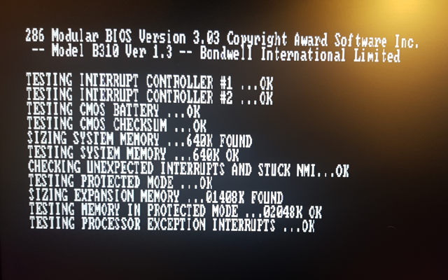
After a fair bit of probing I discovered the reason for this break. When that jumper is in the second position, the entire mainboard set of chips is assigned to a single /RAS line, /RAS0, and then /RAS1 line that went to the second bank of chips then goes to the expansion board instead. Due to how these banks are normally used, that means with the expansion instaled the memory now goes 512kB on the mainboard then alternates with 512kB on the expansion board. So the reason for the memory error at 512kB was that my RAM board was failing for the first 512kB, but worked for he second 512kB on it. More logic probing and reasoning later, I figured out that this was due to the pairs of CAS lines being swapped, as the readback error was showing all 16-bits as not being set. Since I'd assigned the /CAS lines randomly, there was really 4 ways I could have assigned the pairs, and since both bytes were failing that means that both sets were mixed up, CAS0 and CAS1 needed to be swapped and CAS2 and CAS3 needed swapping. I cut the jumpers connecting them and solded a small bit of wire for each to exchange them, re-assembled the laptop, and IT WORKED!
|
2MB of memory in the Bondwell, I had recreated the elusive expansion.
|
I will be uploading the design files to my GitHub shortly after fixing the /CAS pair mixup and missing /WE link. At some point ideally the board would be re-done to mount the ram chips on the bottom side of the board as clearance is tight and even with sightly trimmed down machine pin headers the bottom ram chips press up against the bottom lip of the floppy mount, and the 22uF capacitor is too tall and had to be substituted or a 10uF ceramic I had to hand.
|
Preliminary design files and schematics: Github
The folder gerbers_asmade contains the design files as I made them for my prototype, complete with CAS switch ups and missing /WR connection, besides those these are known to work. The folder gerbers_fixed contains an updated schematic with those changes made but hasn't been designed yet. The schematic contains the fixed version. I do plan on eventually re-doing the PCB properly with the RAM chips on the bottom, and removing the GAL and un-needed jumper pads.